Use Case in Compact Electronic Devices such as Smartphones
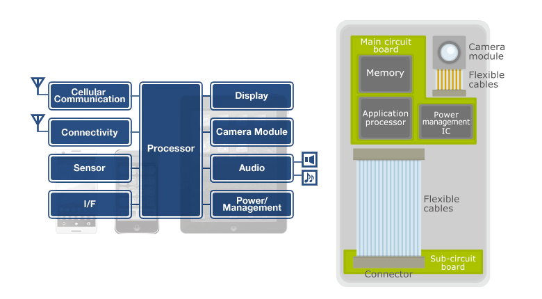
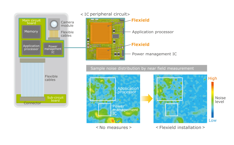
Figure 1 shows the block diagram and basic internal structure of a smartphone. It consists of the main circuit board on which IC circuits such as the application processor and power management IC are mounted, a sub-circuit board which is connected to the display, and the camera module, and they are connected using flexible cables (FPC/FFC).
Figure 1: Block diagram and internal structure of a smartphone
Major causes of noise emission inside smartphones
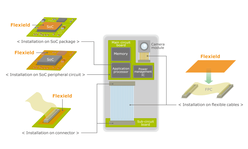
The application processor which is central to the smartphone, and which is becoming increasingly multi-functional, is an SoC (System-on-a-chip) into which multiple ICs have been integrated. The flexible cables and connectors which connect the SoC and the peripheral circuits (power inductors, etc.), as well as the main circuit board and sub-circuit board, are the main sources of noise emission which is the cause of "self-poisoning" in smartphones.
Figure 2: Major places where Flexield is used in a smartphone
Representation of the distribution of noise emission intensity by the near electromagnetic field measurement
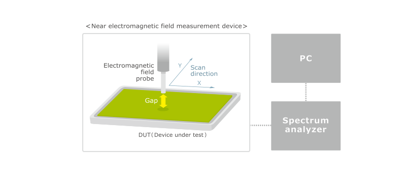
Noise emission consists of electromagnetic waves which are conducted across space through the interaction between the electrical field and magnetic field. However, near the source of noise emission, the electrical field and magnetic field exist independently with either being dominant. This area is known as the near field. In specific terms, the area which is at a distance of less than λ/2π (λ: wavelength) from the emission source is the near field, and the area which is a distance of more than λ/2π is the far field. Since the value of λ/2π is approximately 5cm at 1GHz, in compact electronic devices such as smartphones, it is necessary to understand the distribution of the electrical field and magnetic field in the near field. The near field measurement system is used for this purpose. In this system, an electromagnetic field probe is brought close to the DUT (device under test) such as the printed circuit board, and it scans the device while maintaining a fixed gap, and the data obtained is used to represent the distribution of noise intensity (Figure 3). Simulation technology, which is one of the core technologies of TDK, is used as a solution for various noise problems such as the "self-poisoning" problem.
Figure 3: Configuration of a near electromagnetic field measurement system
Power inductors are also a cause of noise emission
Figure 4 shows an example of the distribution of the magnetic field intensity of the IC peripheral circuits of the main circuit board in a smartphone, measured using the near electromagnetic field measurement system. The area with high noise level is shown in red, while the area with low noise level is shown in blue. In the absence of any measures, the red area is widely distributed around the application processor and power management IC, but when Flexield is installed, the noise level is considerably reduced. Since the noise is emitted not only from the ICs, but also from the power inductors, installation of Flexield in the IC peripheral circuit is an extremely effective noise suppression measure.
Figure 4: Example of the effectiveness of noise suppression in the IC peripheral circuit of the main circuit board
The cabling and wiring pattern functions as an antenna which emits noise
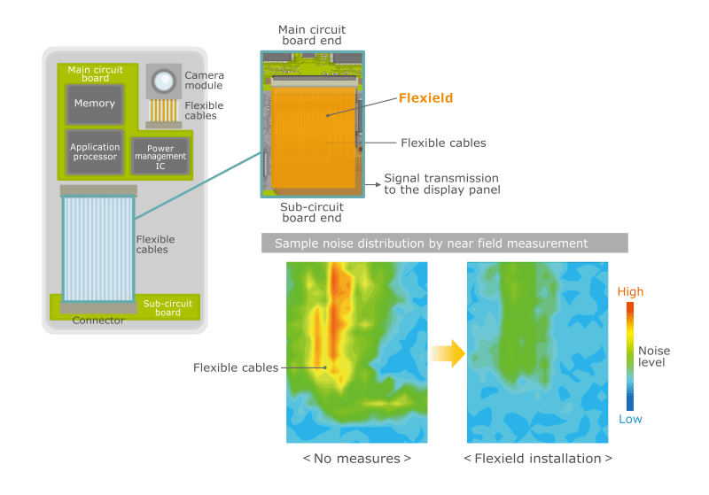
Since Flexield is thin and flexible, it has the advantage of being able to be easily attached even to flexible cables. By installing Flexield, there has been considerable suppression of intense noise.
Figure 5: Example of effectiveness of noise suppression in flexible cables
