Official distributor of

Europe GmbH for ferrites in Europe
Significantly more efficient with improved materials and geometries

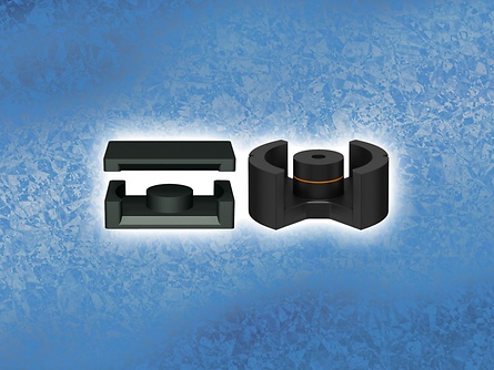
Apart from miniaturization, improved efficiency is the most important development goal in the design of power supply units. Every tenth of a percent counts. Apart from the power semiconductors, ferrite cores are the decisive factor for efficiency. TDK has developed a new ferrite material and improved geometries for the core designs.
All types of power supplies require ferrites which, in a wide variety of core designs, then become the basis for inductors used for energy storage and transformers for power transmission and galvanic isolation.
Although efficiencies in excess of 98 percent are already being targeted today, developers are still struggling to gain every tenth of a percent, particularly in the case of high powers, in order to further increase efficiency, while at the same time miniaturizing components to save space and weight.
New wide bandgap semiconductors such as GaN and SiC are facilitating further advances, because they can switch higher frequencies with higher slew rates and lower losses. This means that, in principle, it is possible to use considerably smaller inductors and transformers, or to handle higher power ratings with a component of the same size. The disadvantage is that conventional existing power ferrite materials are not designed for frequencies in the MHz range, where they exhibit greater losses than at lower frequencies.
New PC200 material offers high efficiency at up to 4 MHz
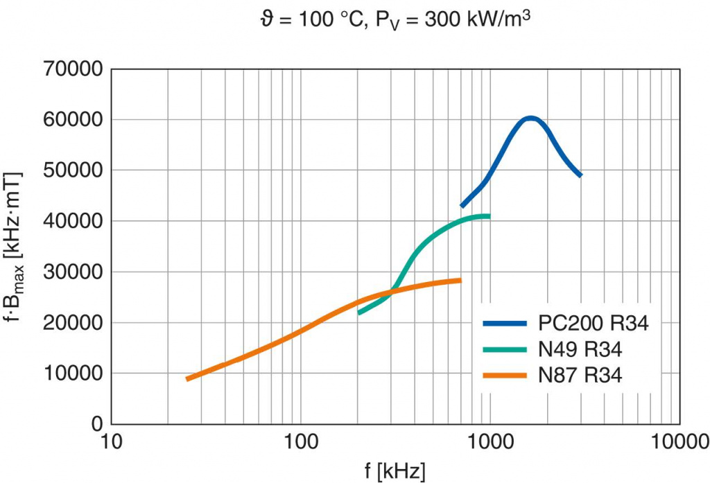
In order to be able to exploit the advantages of the new semiconductors, TDK has developed the new PC200 ferrite material based on MnZn that is designed for the frequency range between 0.7 MHz and 4 MHz. The maximum transmissible power is reached at a switching frequency of between 1.8 MHz and 2 MHz and an operating temperature of 100 °C. The Curie temperature is in excess of 250 °C and the PC200 ferrite material is particularly suitable for transformers based on ring or planar core topologies. Figure 1 shows a performance comparison between PC200 and conventional materials.

Figure 1:The new PC200 MnZn ferrite material offers its optimum performance at a frequency of about 2 MHz and is thus ideally suitable for topologies of power supplies that are based on new wide bandgap semiconductors such as GaN and SiC.
70 percent less loss due to distributed air gaps
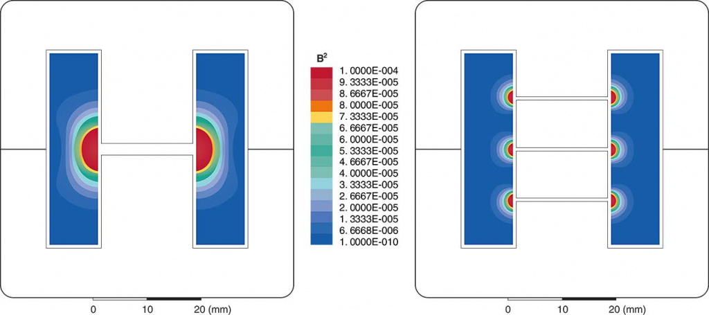
The use of single air gaps in ferrite cores is a common technique today for delaying the core saturation and thus increase the performance. These relatively large, single gaps however result in a higher fringing flux effect, leading to additional copper losses, particularly at high frequencies. With new geometries and the core manufacturing technique of distributed air gaps, TDK is the first ferrite core manufacturer to offer an elegant solution for reducing electromagnetic emissions and thus heating (Figure 2). By arranging the gaps in the center post, the magnetic field emissions to the environment is effectively prevented.

Figure 2: Due to the identical distributed air gaps (right), the power losses (red areas) can be significantly reduced compared to the conventional solution with just one gap (left). Solutions with three identical air gaps offer the best cost/performance ratio when used in applications with high frequencies.
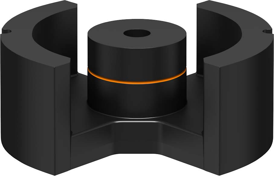
Different sized cores are available with three distributed air gaps in E, EQ, ER, ETD, PM and PQ core designs, and with all EPCOS power materials. Solutions with three air gaps (Figure 3) offer the best cost/performance ratio for applications in which the switching frequency is 2 or 3 times higher than the original frequency. This enables the losses to be reduced by up to 70 percent. Apart from standard solutions, a customer-specific number of air gaps can also be implemented.

Thanks to the new PC200 ferrite material and the advanced core geometries, it is now possible to make maximum use of the advantages offered by the new semiconductor technologies, while at the same time satisfying the demands for both higher efficiencies and miniaturization.

